Electronics production
This week was electronic production week. I thought I might make a new, easier board for the humidity sensor, but in the end I could make it work with the one I designed 2 weeks ago.
Group assignment
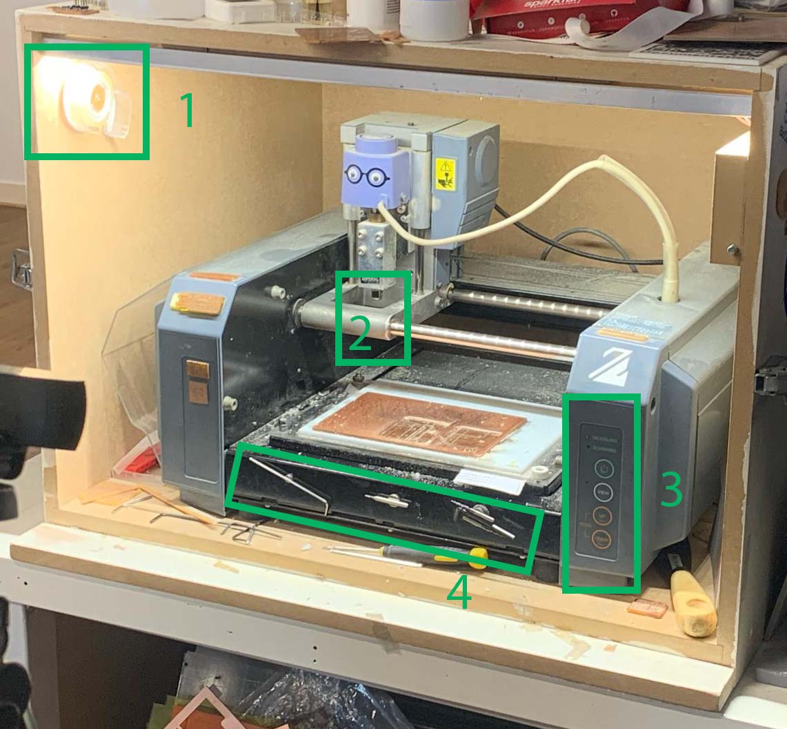
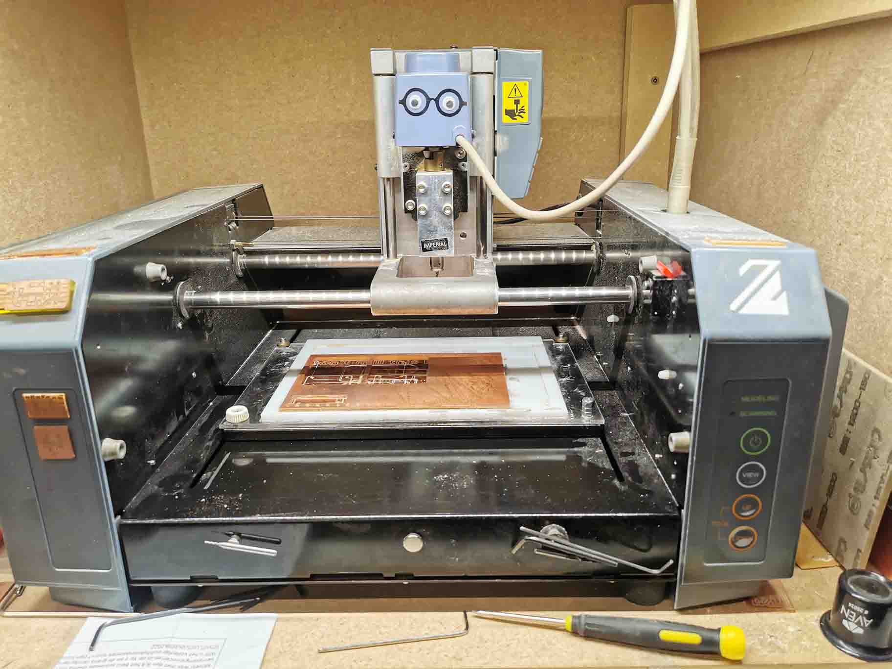
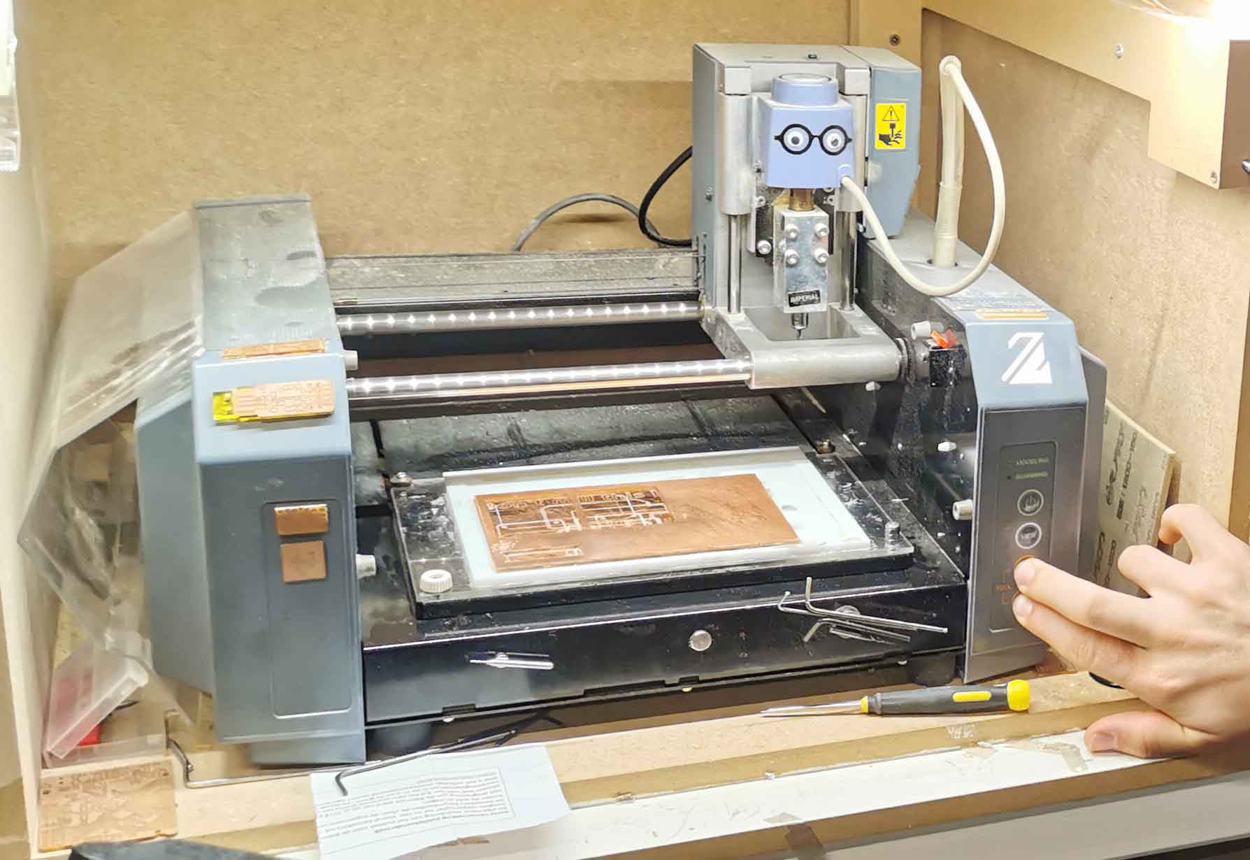
Here is our googlie eyed milling machine. It is a MDX-20. In the picture above you can see:
1: The double sided tape. Always return to the hook - or you will owe the rest of the team cookies.
2: The milling head, where the bit gets attached.
3: The control panel consisting of ON/OFF, VIEW, UP and DOWN.
4: And finally the toolstation. There are small tools keeping the most important/common tools in place.
We first removed the plate from the bed.
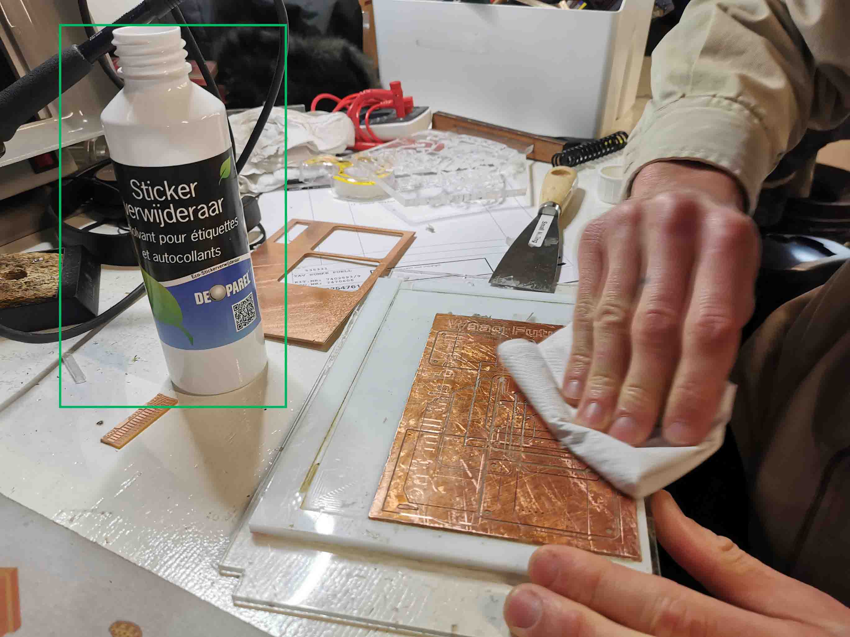
Used a spatula to get the coppercoated plate off the sacrificial layer.
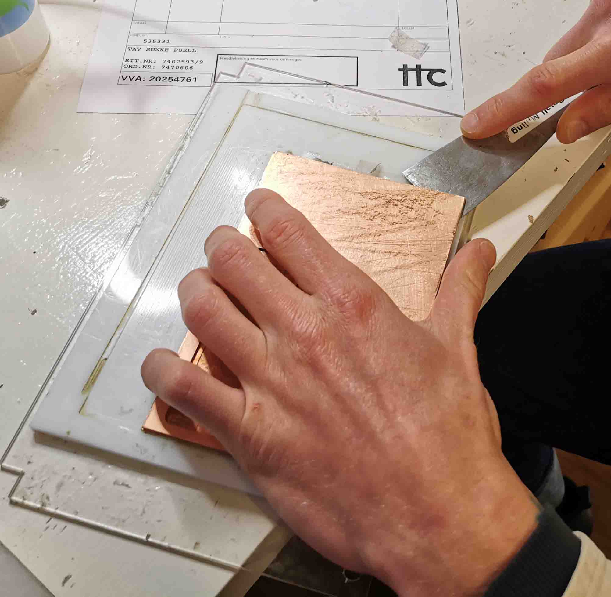
It was attached with double sided tape:
We cleaned the sacrificial layer wit anti-sticker-stuff. It was important to first make sure to get all the tape off and then after cleaning it feel for any leftover glue. And finally dry it properly. If it has not been properly dried then the tape in the next step will not attach.
Then we did the same to the top plate.
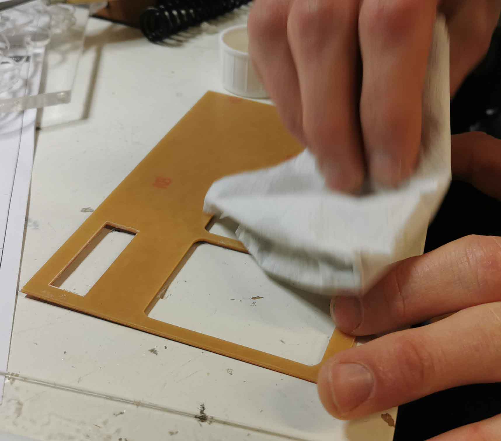
And attached new double sided tape. Making sure to not overlap tape since this will make the height of the plate uneven for when we are milling.
Then we mounted the baseplate back onto the machine, securing it in place.
To operate the machine we are using mods:
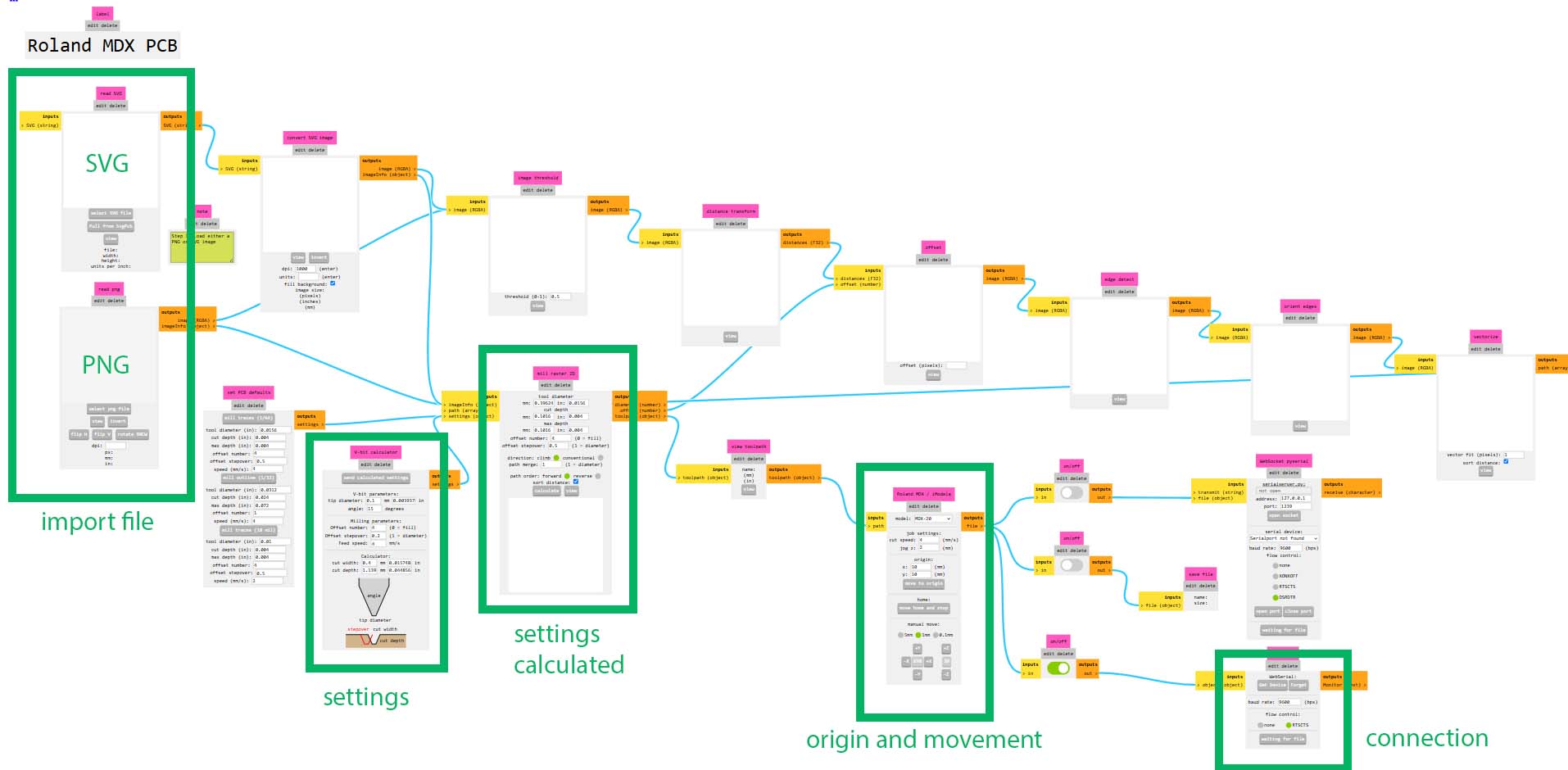
The files we were using was already on the machine as pngs since Henk had just showed us how to do this. So we used the lower left panel to iport our files.
We were using a 0.25mm bit, which actually creates a 0.4 trace, because of the depth of the bit and the 20 degree angle it slopes on. For teh file we were cutting around we did an offset of 4. This means that it will go 4 rounds outside of the chose trace. If we wanted everything extra removed we should have chosen 0 (fill). But we did not need this here. Just good to know for later.
Here are our setting:
tip diameter .25
angle 20 degrees
offset 4
stepover .5 (half of the diameter)
feed 4
after hitting calculate the machine translated the values and we could here adjust them. These are the values the machine will use.
cut width .4 mm
cut depth .0762 mm / .003 in
max depth .0762 mm / .003 in
direction climb
path order forward
Sort distance ON
We generated toolpaths based on these values. Erwin had a tip for us. Once the toolpaths are generated the 3D viewer should pop up. If it dies not, something may be wrong. I think this is not always the case. I noticed that if the 3D viewer window was always open then a new one does not pop up. But it is still a good rule of thumb to double check that nothing is wrong.
We moved the milling head to the origin point and stopped it a bit above the copperlayer. Then loosened it until the bit was touching the plate.
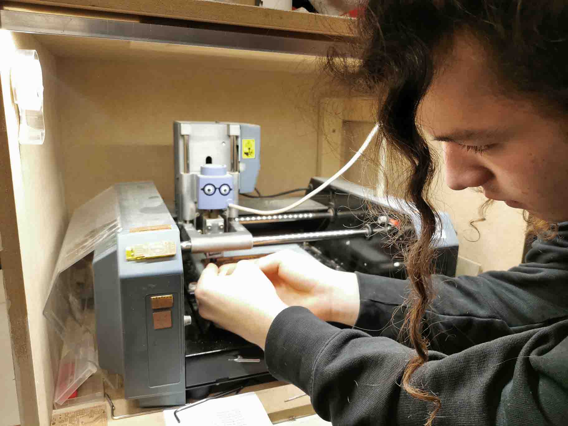
Like this. Looks good. Remember to tighten the screw again.
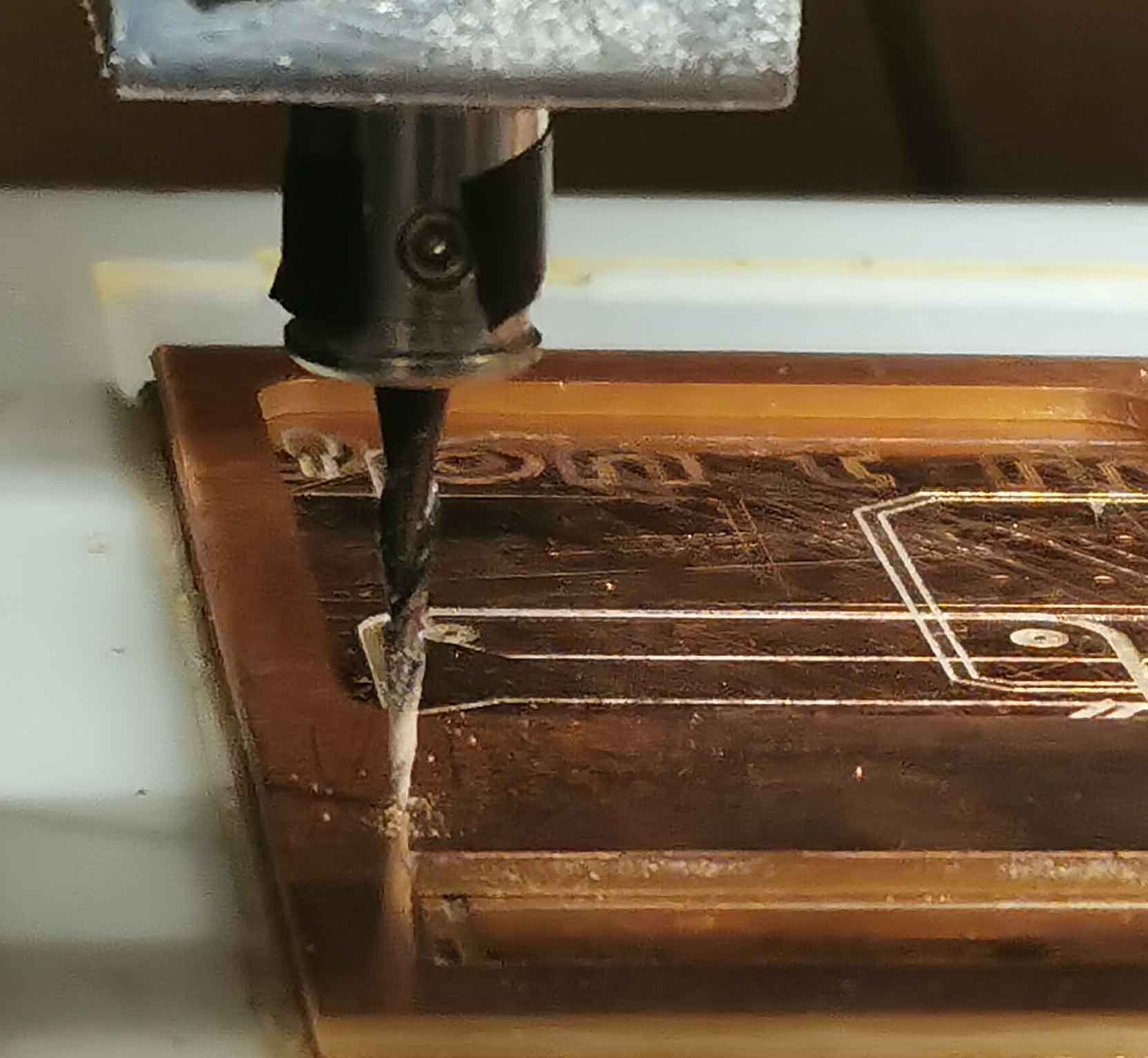
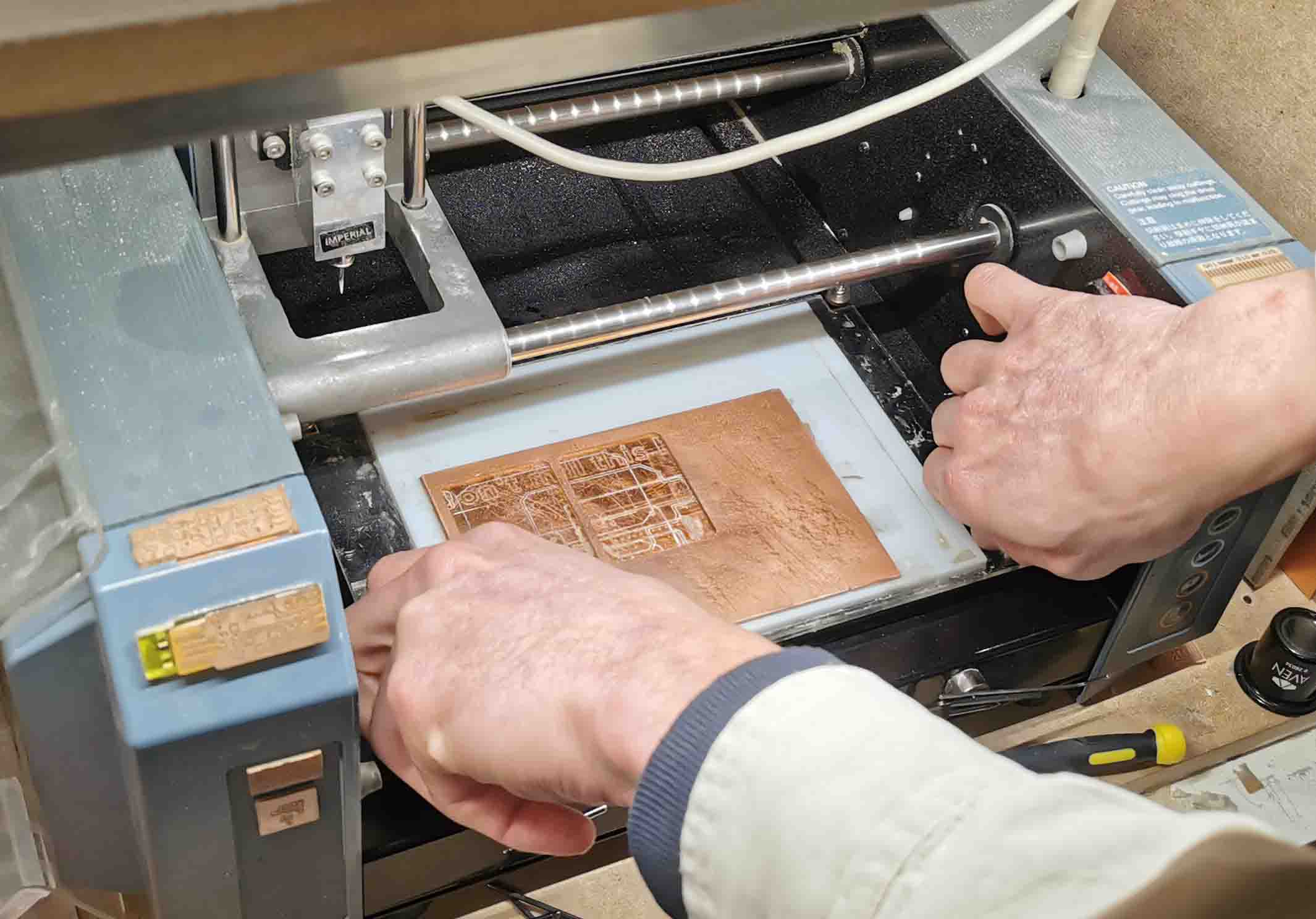
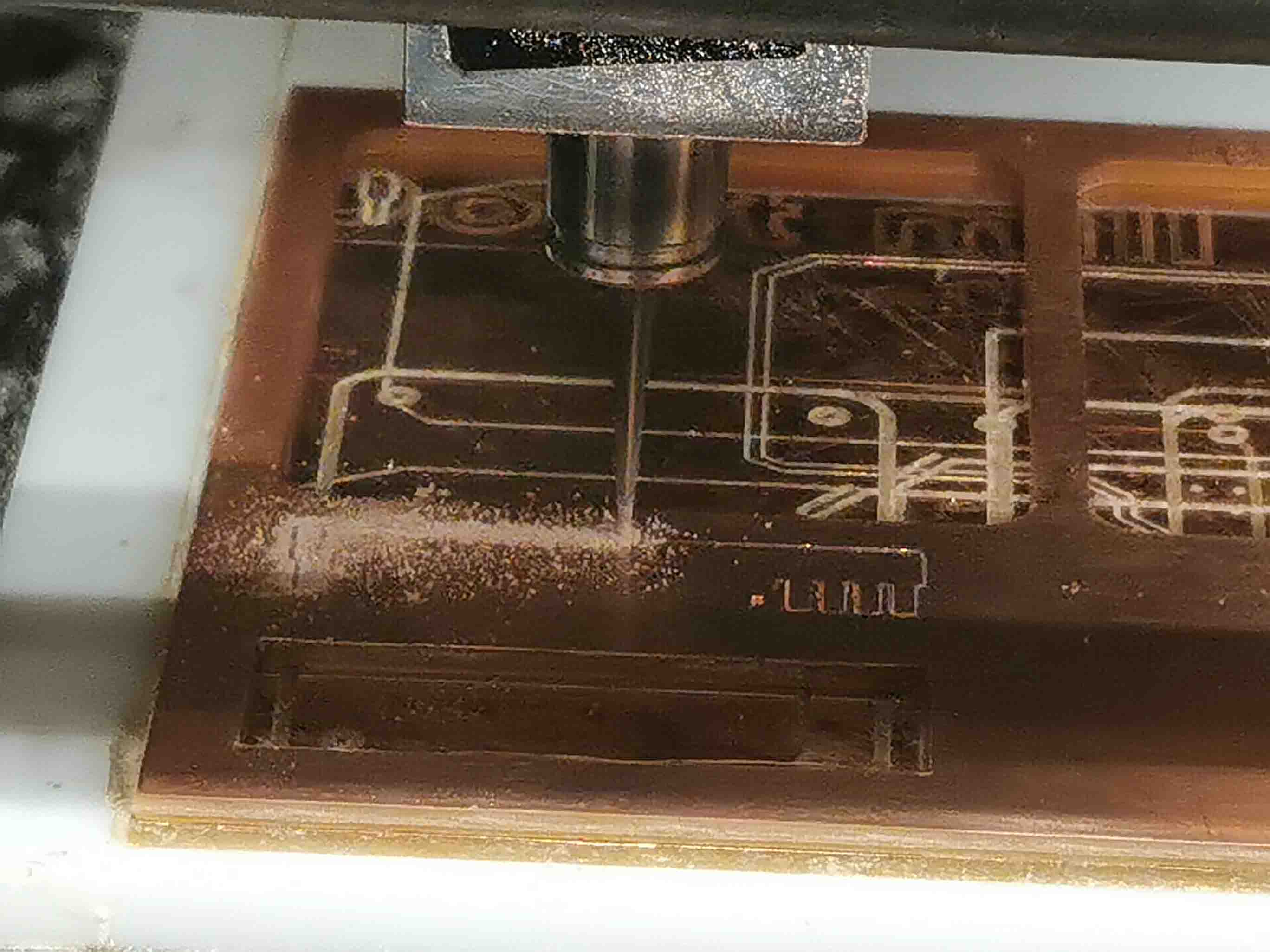
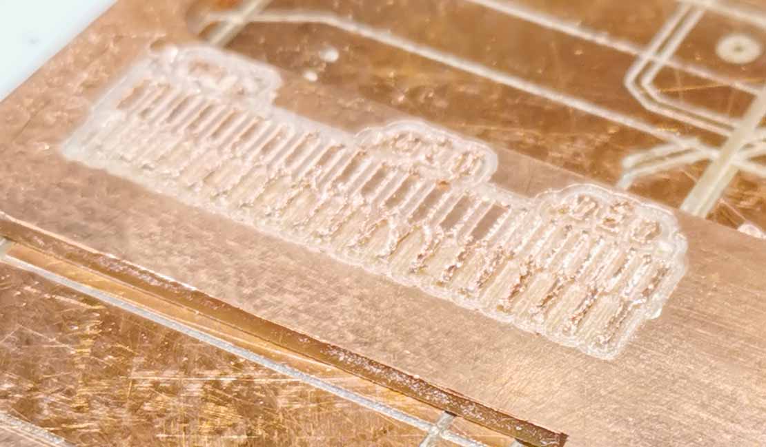
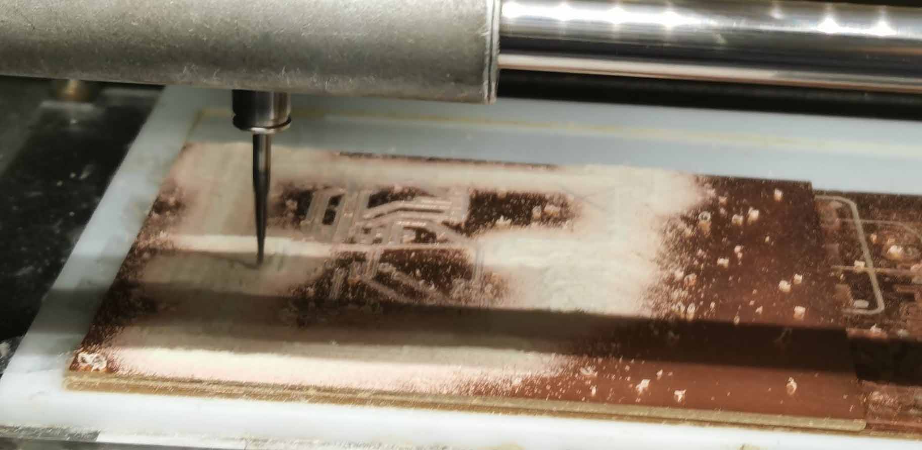
Using the Webserial we sent the file to the machine and started milling. To pause it we pressed view. And inspected the path using a magnifyingglass. As seen below we were not cutting all the way through and were only etching the copper. THis is not good. We needed to adjust the cutting depth.
We reset the machine by unplugging the usbcable from the computer and pressing UP and DOWN for 10 seconds.
It took a few tries but in the end we got the right depth.
With a cutting depth of 0.101 mm we got through.
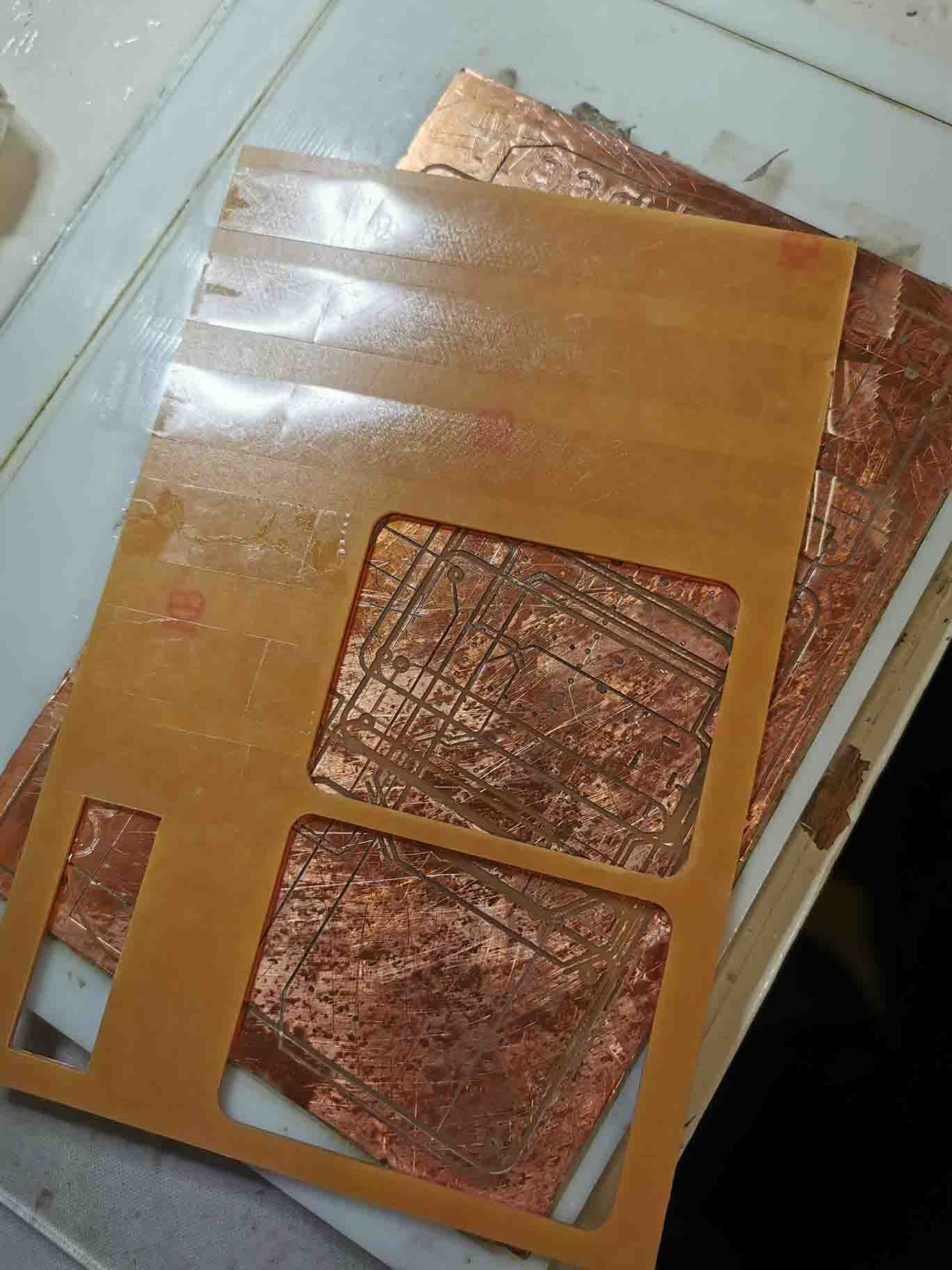
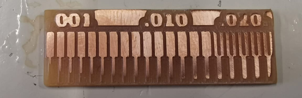
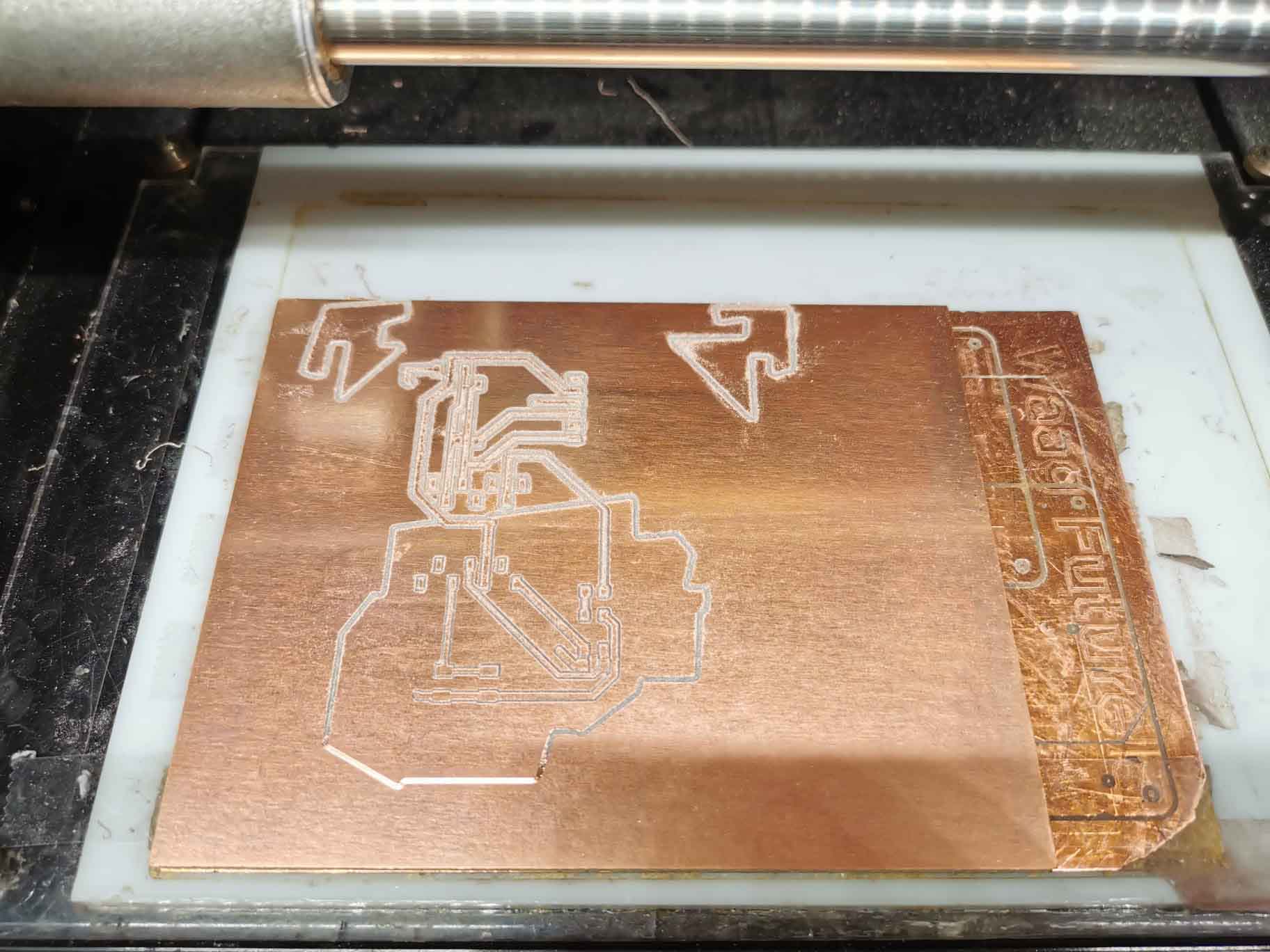
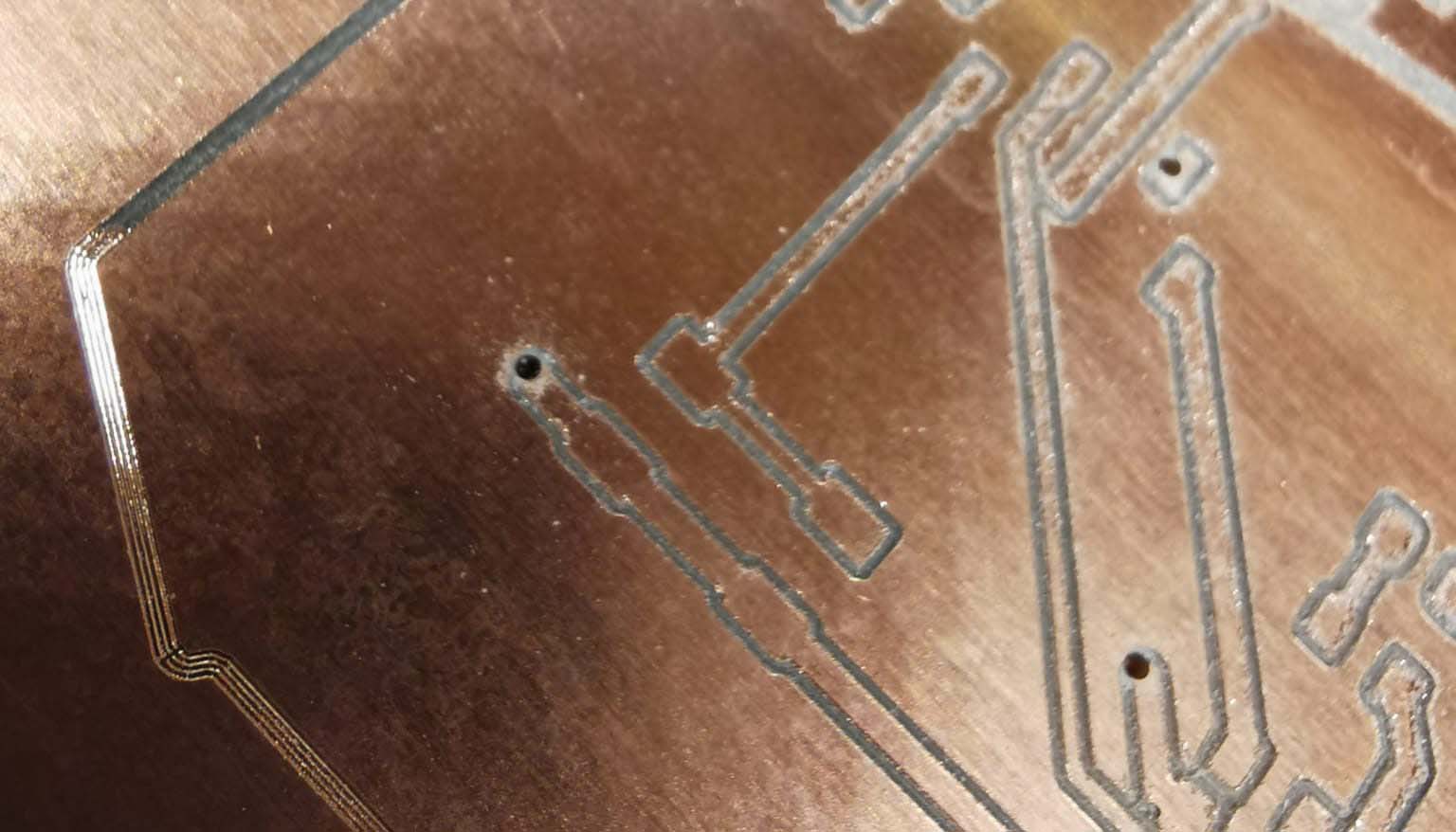
Here is the result of having milled the inside of the board:
On to the outline. Here there was some adjustments needed.
offset 1
Cut depth 0.3 mm
Max depth 1.55 mm
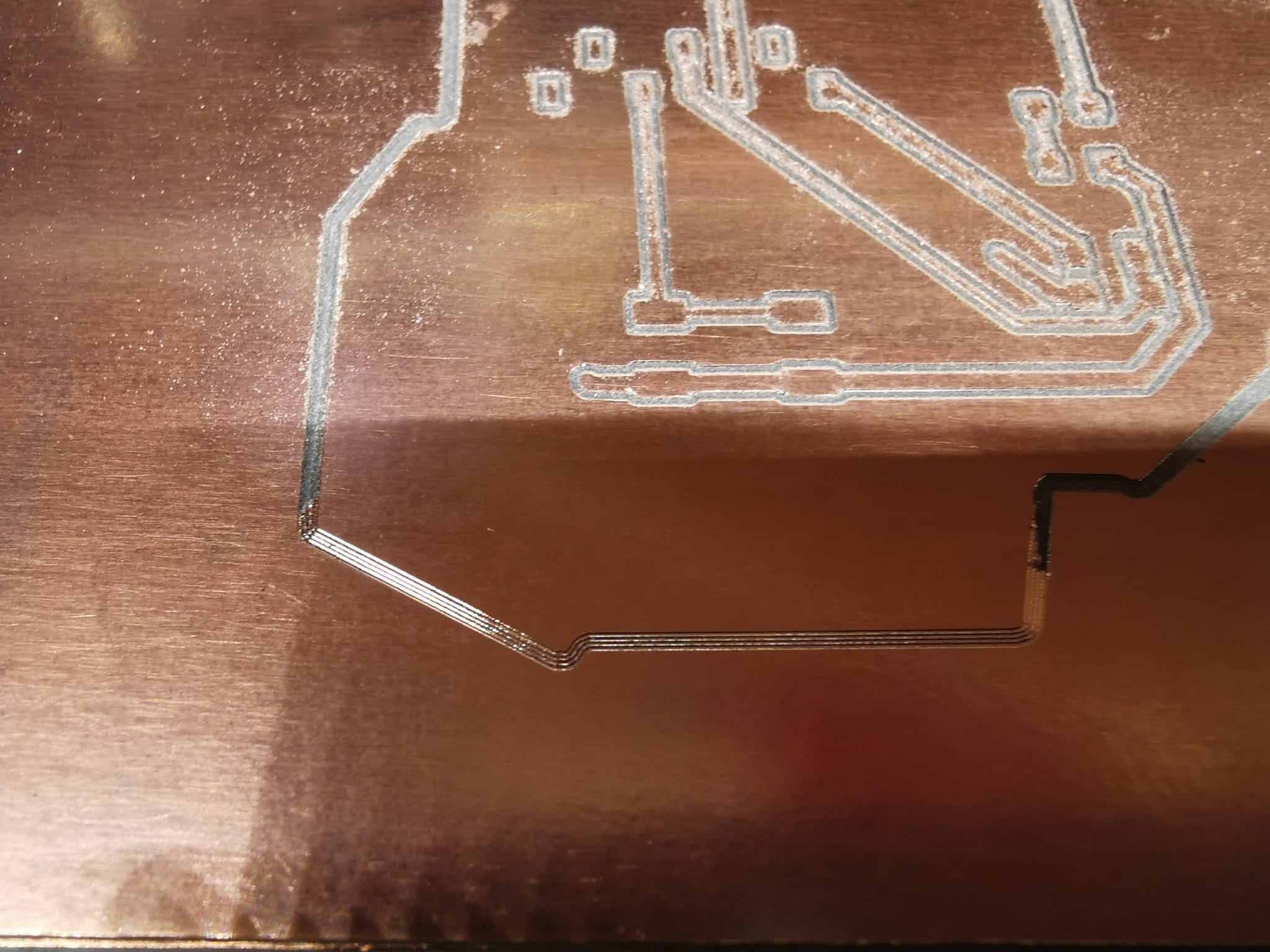
We went a bit crazy with sanding and ended up removing parts of the copper lines when we were done.
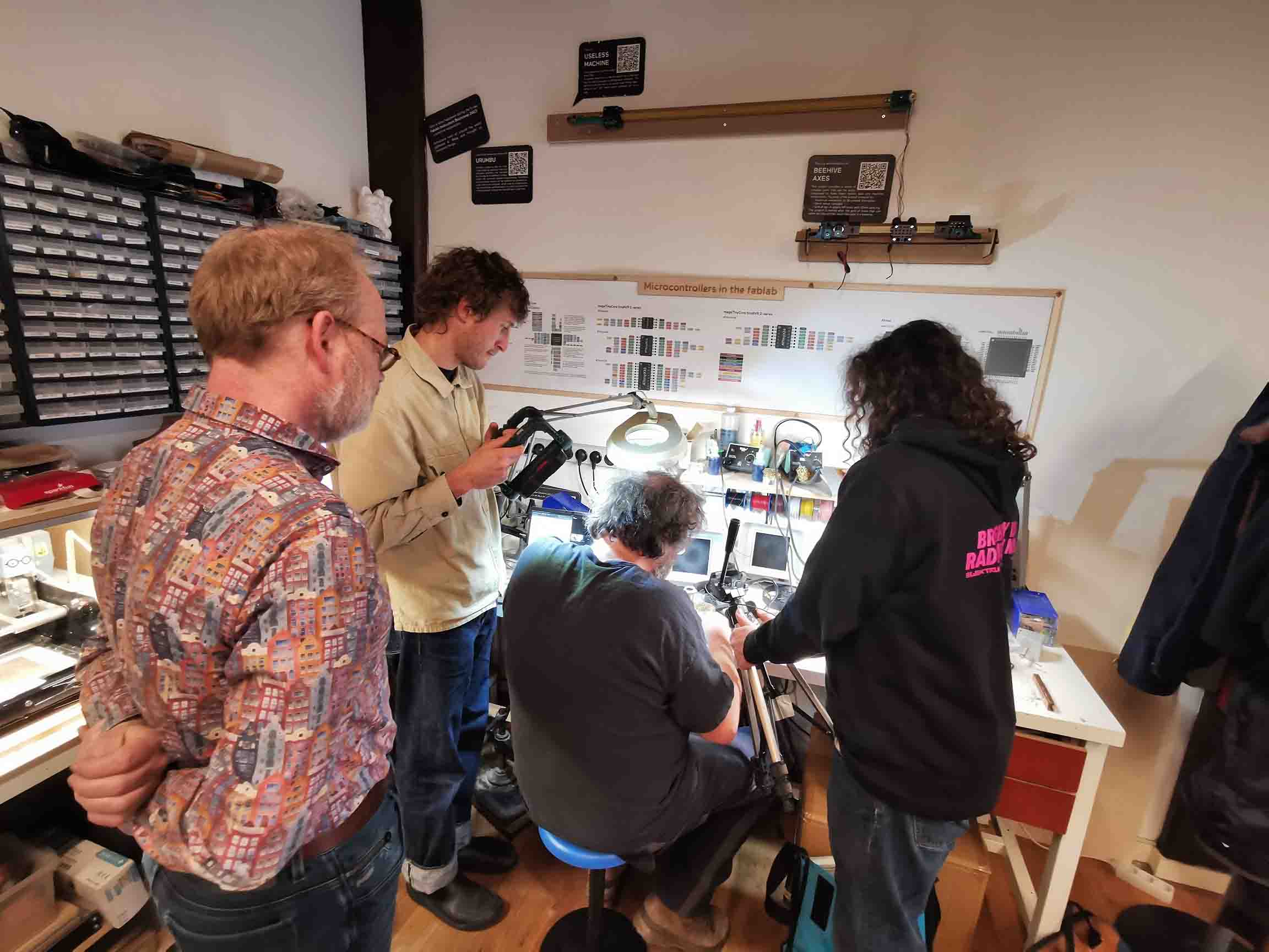
At the end of the day Henk gave us a quick intro on how to solder. We had Patric online and since the components are very small this turned into a whole production with Sam acting as cameraman and Dylan focusing on the light.
My own board
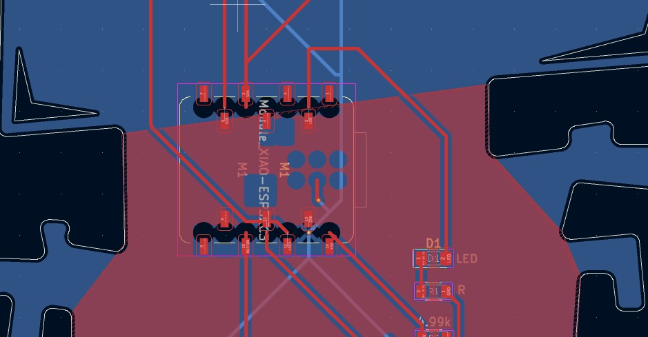
This week I wanted to mill the board I designed a few weeks ago. But I quickly realised that I had made a terrible mistake. I was grounding all the components on the back of the board, but I ahd also put in header pins that went trough the board. Meaning that everything was connected!
I had to update the footprints and rewire the board. I first thought I could not use the back, but it worked out.
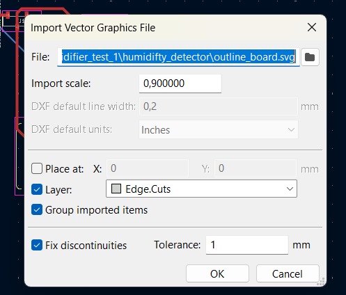
My next problem was that it was quite a big board I had designed, so I wanted to make the outline smaller. It was not as simple as to just click and drag to change the size. SInce the edgecut is a bunch of small points. I had to delete and re-import the edge cut. Luckily there is a parametere called Imprt scale witch allowed me to import it just slightly smaller. I did .9 import.
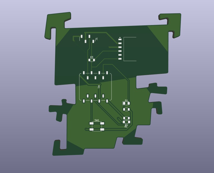
This is what my new board looked like. I was happy with this.
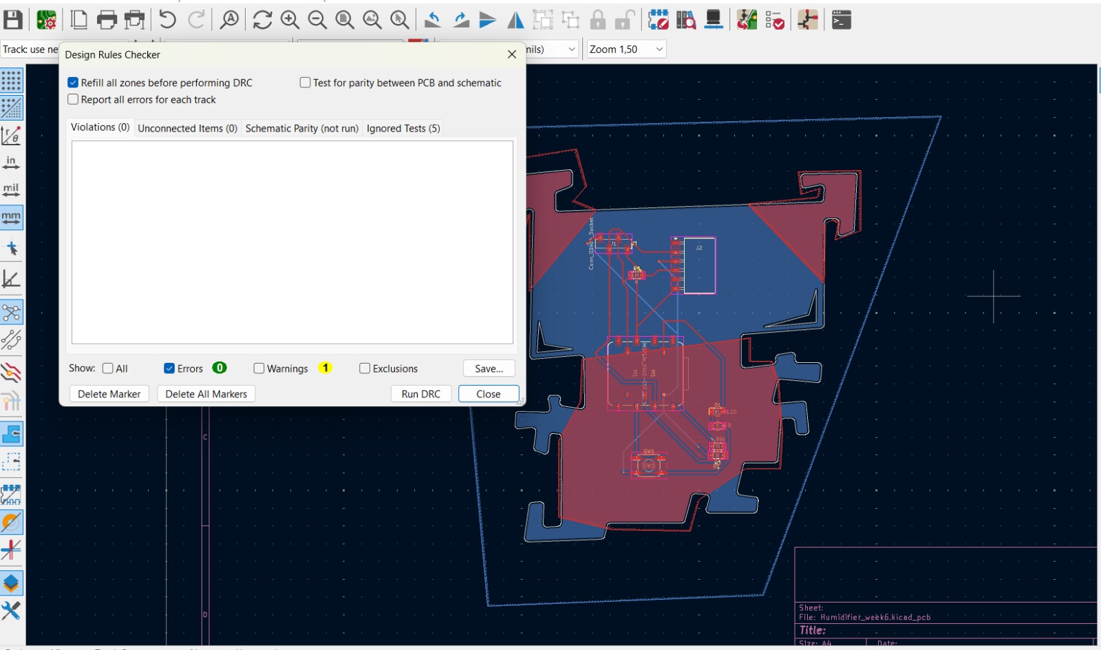
Since I had remodeled it I did a Design Rule Check.
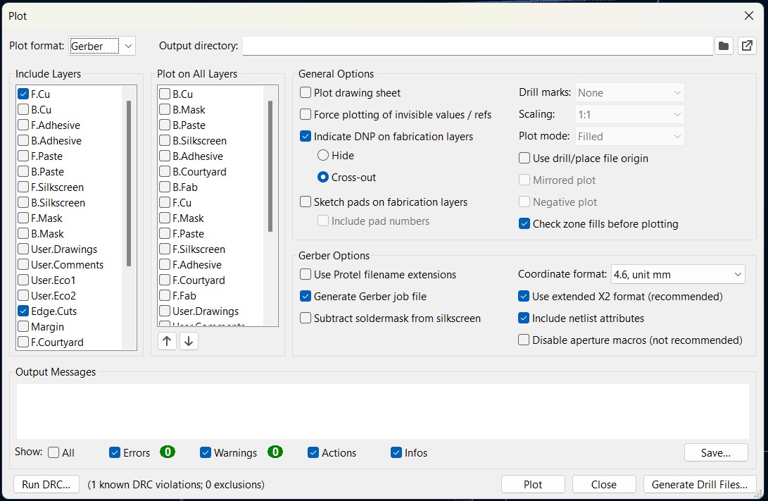
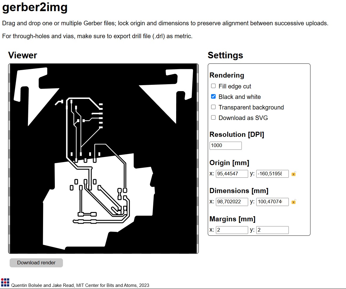
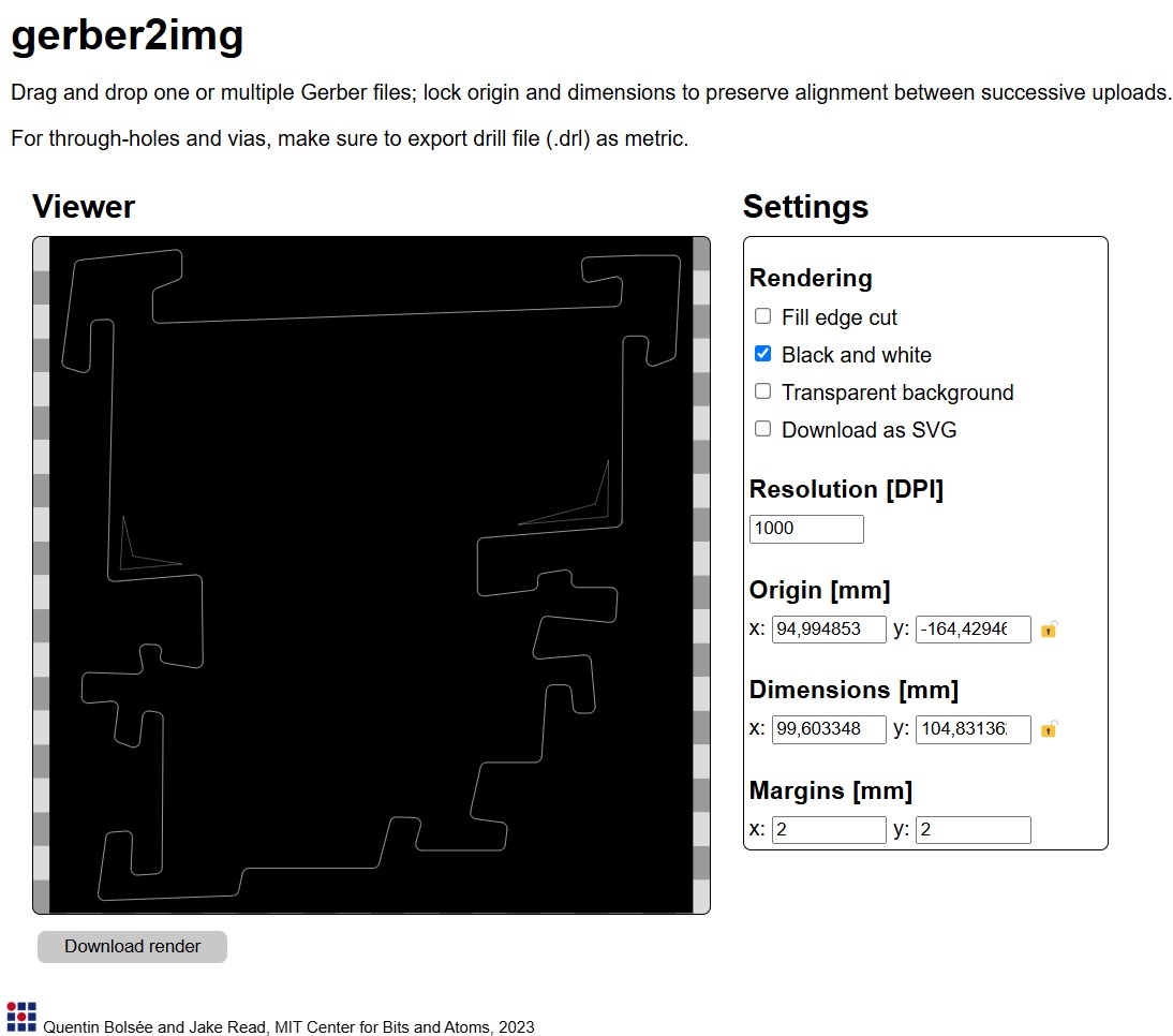
I exported the Front Copper Layer and Edge Cuts as gerber files.
Imported them in the gerber2img converter. One thing to note: remeber to lock teh dimentions and origin. I did this later on but do not have images of that.
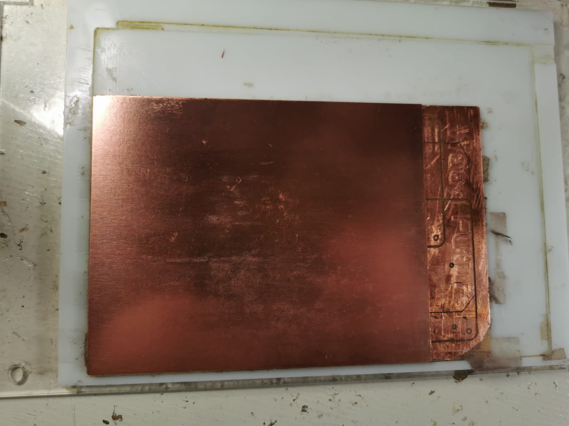
I taped down a 2 layer copper plate.
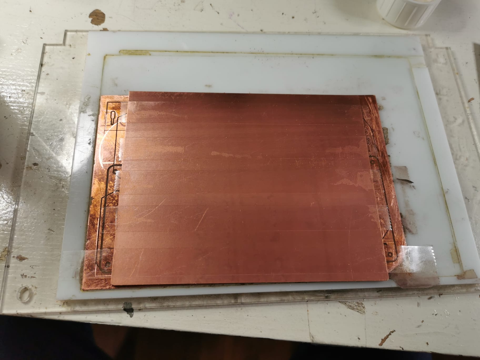
Added it to the sacrificial layer.
I then milled the traces on the board. Really happy to see it take shape.
I noticed while it was milling that the bottom part of the board was only etched, but since this line is only for aestetics and nothing functional I didn't do anything about it.
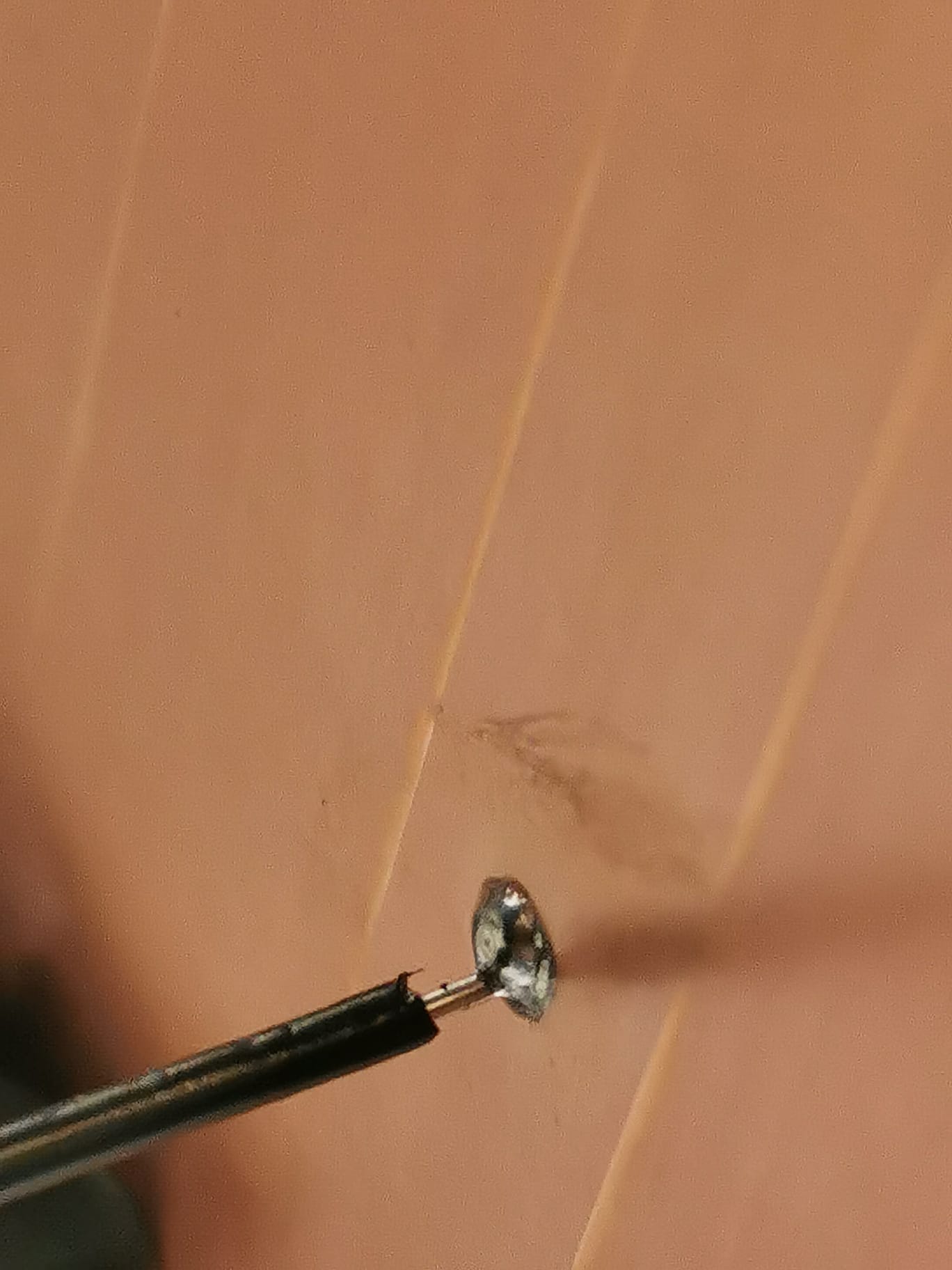
Milling the holes was a bit of a pain. I couldn't figure out how to export the right file to get the holes in gerber, but in the end I saw that Quinten had written on the gerber2img page that for vias you can import the drl file and then it worked. I also had to invert the image and change the bit to the .8mm with no angle.
I was again very confused at this point, but luckily Henk helped me. My holes in the file was the wrong size. We had to tell the machine it had a .2mm bit and then start it. The holes were milled with a .8mm bit which was good for what I needed.THe placement of the wholes were almost perfect.
After that it was time for the outline. I got confused by mods again and Henk helped me again. I had left the offset at 4, but it needed to be 1. The cut depth needed to be .2 and the max depth 1.55 mm.
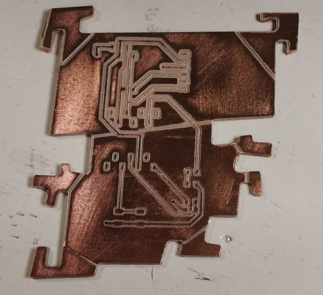
Here is the finished outline! Im super happy with it!
I completely forgot about Henk telling me we had something to put in the holes, and he was out for a smoke so I used wire and tin to connect the grounf pins to the back of the board.
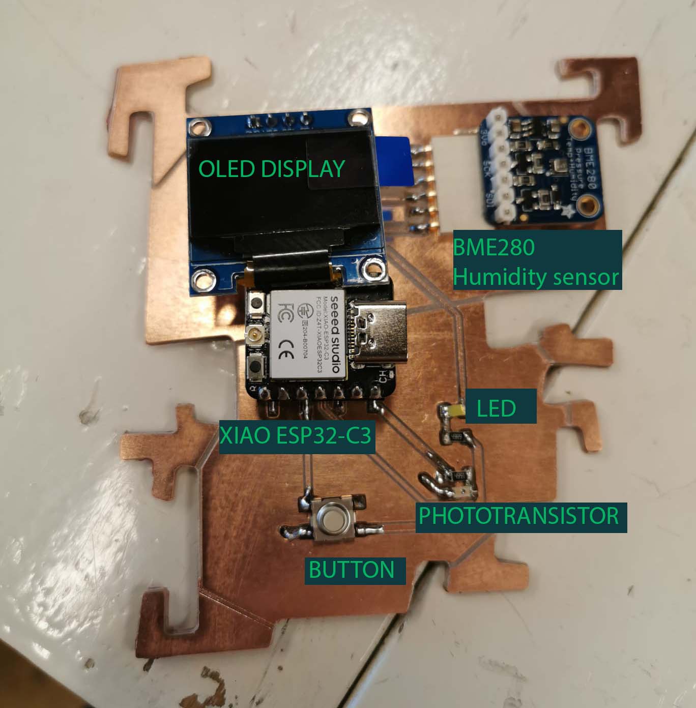
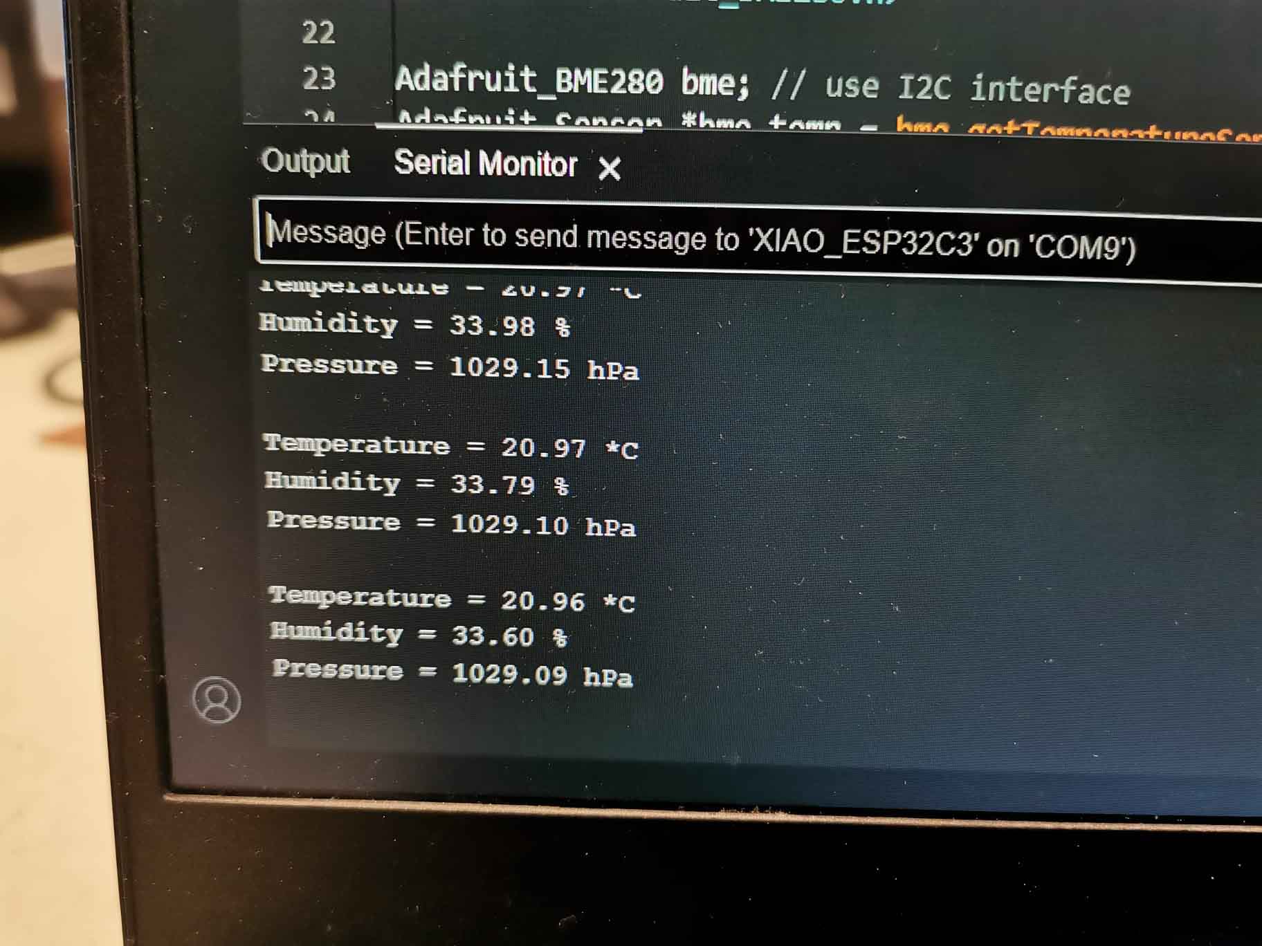
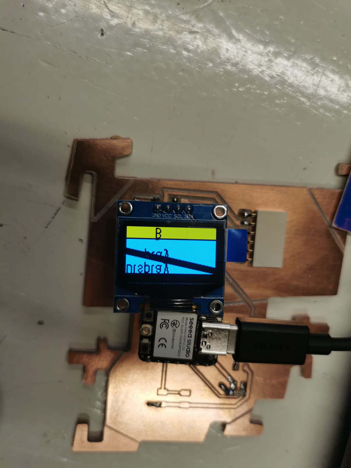
Once the sockets for the microcontroller, BME280 and the OLED display was in place I went on to test them.
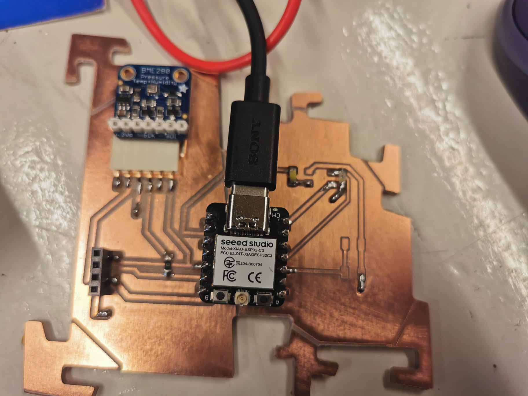
The humidity sensor works!
SO does the OLED diplay!
I soldered on the phototransistor, LED, button and the resistors and this is the final board:
This week was pretty nice I think. At the beginning I though I would not be able to mill the board from a couple of weeks ago because I imagined that it would be too tricky and that I had made some big mistakes. I had make some routing mistakes, but could fix it with not too much trouble.
I have to remember to not put any components through the board if I intend to ground on the bottom copper layer. And I definitley think the small copper cylinders henk was proposing would have looked neater then what I did with the wires.
When it comes to Mods I feel more comfortable using it. I think I understand most of what I did not understand before. With offset and millingbit size. I still find it a bit confusing, but hopefully as I use it more it will feel less ailien. I think I'm getting thrown off by how it looks aswell. Next time I will check that all my sizes in the kiCad file matches the milling bits I'll be using.